

The Atomic Force Microscope (AFM) was established in the central laboratory of Lorestan University.
 Oct 28, 2015
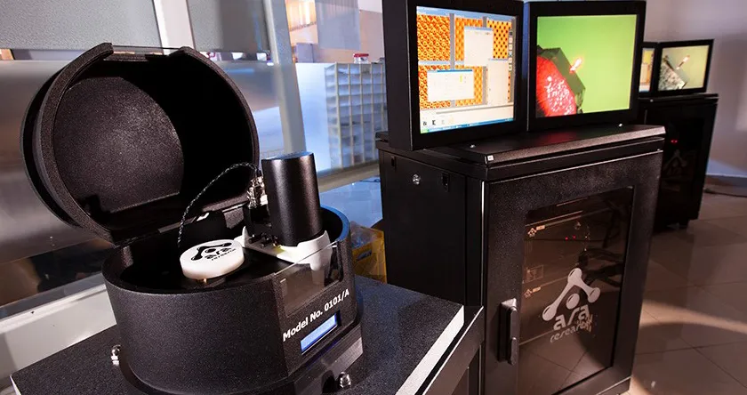
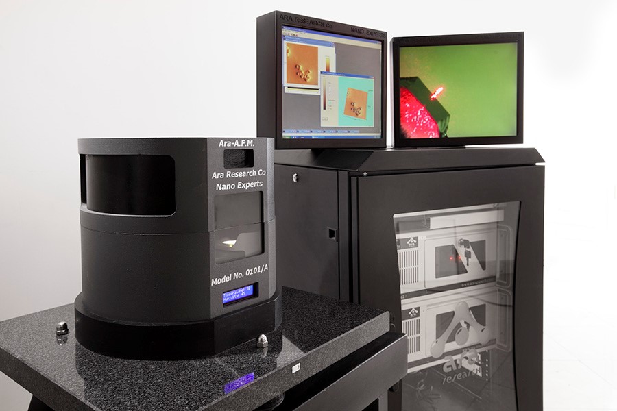
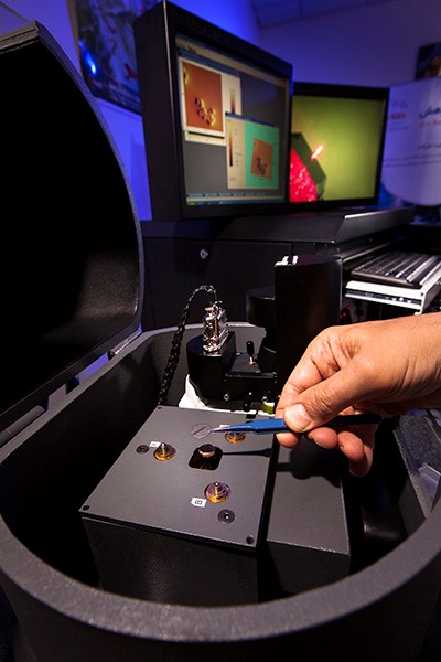
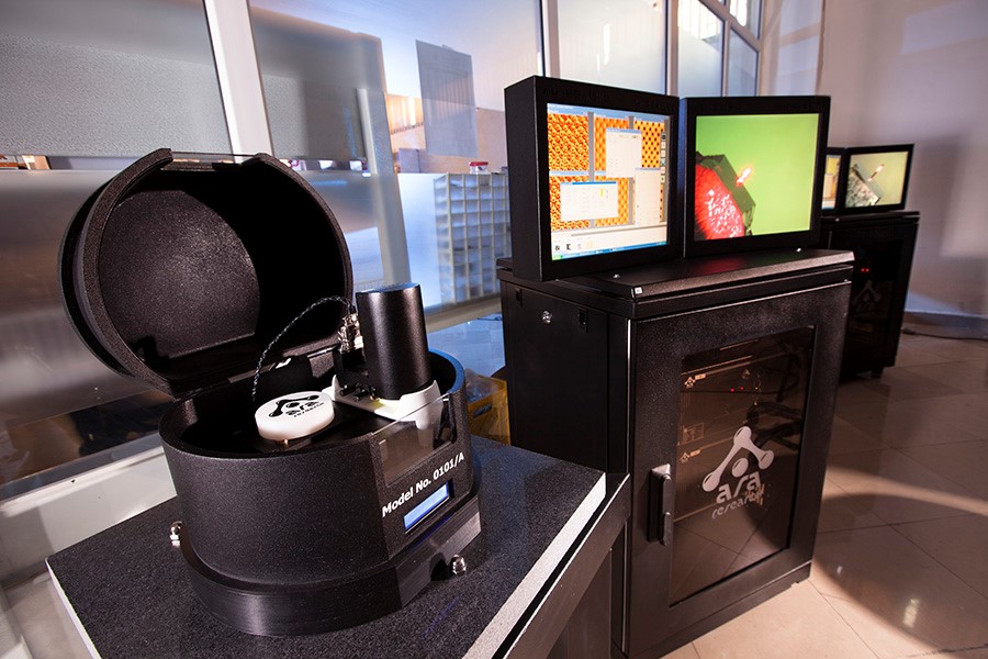
The Atomic Force Microscope (AFM) has been installed in the central laboratory of Lorestan University and is ready to provide services to researchers both within and outside the university. This microscope is manufactured by the Iranian company Ara Pazhouhesh (Full pluss model) and was purchased from the third exhibition of laboratory equipment made in Iran with the assistance of the Vice Presidency for Science and Technology.
Working Principle:
To observe objects and samples with very small dimensions, on the order of small molecules and atoms, conventional microscopes cannot be used; because these samples have nano-scale dimensions, and conventional microscopes are not capable of showing nano-scale dimensions and show up to the micrometer scale. Therefore, to see nano-scale samples, more precise and advanced tools must be used. One of these tools is the AFM.
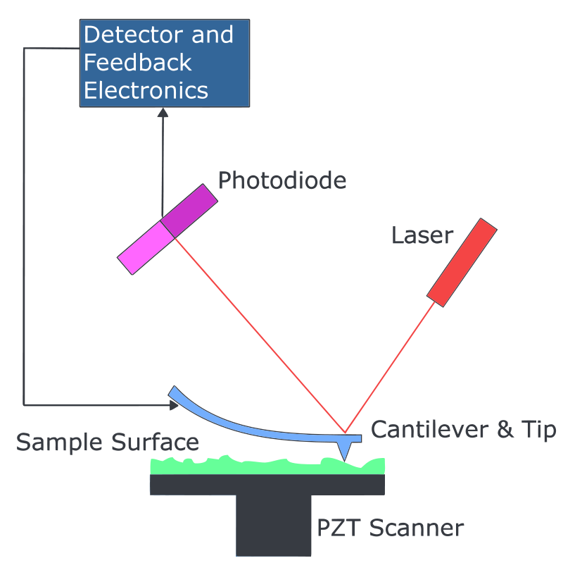
We know that all objects, no matter how smooth and polished they appear, still have irregularities and roughness on their surface. For example, the surface of glass appears very smooth and polished, but if we look at it on a very small scale, we will see that the surface of the glass is full of irregularities. The function of the atomic force microscope is to show these irregularities and measure their depth. The figure below shows how an atomic force microscope works.
The atomic force microscope has a tip that is placed on a cantilever. This tip, which is usually a single diamond atom, moves on the surface of the sample, and the cantilever bends due to the attractive or repulsive force between the atoms of the surface and the tip. By bending the cantilever, the reflection of laser light on the photodetector is displaced. In this way, the displacement of the cantilever tip can be measured. Since the cantilever follows Hooke's law in small displacements, the interaction force between the tip and the sample surface can be obtained from the displacement of the cantilever. And from the force between the atoms of the sample surface and the probe, the distance between the tip and the sample surface, or the height of that part of the sample, can be obtained.
There are three types of contact between the tip and the sample surface:
Contact Mode
In this mode, the microscope tip is in weak contact with the sample, and imaging is done by measuring the deflection of the tip (by the repulsive force between the tip and the sample).
Non-Contact Mode
In this mode, there is no contact between the microscope tip and the sample, and imaging is done from the attractive force between the tip and the sample.
Intermittent Contact Mode (Tapping Mode)
This mode is similar to the non-contact mode, with the difference that in the intermittent contact mode, the oscillating tip of the cantilever gently collides with the sample, and the oscillation amplitude is much larger than the non-contact mode. In this method, imaging is done using the oscillation amplitude of the cantilever. This device can be used in vacuum, gas, and liquid environments. The scanning range of this microscope is from 1nm to 100 µm and has atomic and molecular accuracy.
Applications of the device:
Advantages:
1- It can provide a three-dimensional image of surfaces in addition to a two-dimensional image.
2- The sample does not need special preparation such as gold or carbon coating.
3- It can be used for conductive, semiconductor, and insulator samples.
4- Operation in non-vacuum conditions
5- No limitation on the type of sample (unlike SEM, TEM, STM)
6- Suitable laboratory size (unlike SEM, TEM)
7- Suitable for imaging aerobic living samples